Voltage Amplifier PD200 - Test Bench
Table of Contents
- 1. Requirements PD200 Expected characteristics
- 2. Voltage Amplifier Model
- 3. Transfer Function measurement
- 4. Noise measurement
- 4.1. Measurement Setup
- 4.2. Model of the setup
- 4.3. Quantization Noise of the ADC
- 4.4. EG&G - Amplifier noise measurement
- 4.5. Femto - Amplifier noise measurement
- 4.6. PD200 - Low frequency noise measurement
- 4.7. PD200 - High frequency noise measurement
- 4.8. 16bits DAC noise measurement
- 4.9. Noise of the full setup with 16bits DAC
- 4.10. 20bits DAC noise measurement
- 4.11. Noise of the full setup with 20bits DAC
- 4.12. PD200 Amplifier noise model
- 5. Output Impedance
- 6. Comparison to other commercial amplifiers
- 7. Conclusion
This report is also available as a pdf.
\clearpage
The goal of this test bench is to characterize the Voltage amplifier PD200 from PiezoDrive.
This document is organized as follows:
- Section 1: the requirements for the amplifiers and the characteristics of the PD200 amplifiers as advertise in the datasheet are listed.
- Section 2: a very simple amplifier model consisting of a transfer function and a noise source is described.
- Section 3: the transfer function from input voltage to output voltage is identified.
- Section 4: the power spectral density of the amplifier’s noise is measured
- Section 5: the output impedance of the PD200 is estimated
- Section 6: the characteristics of the PD200 amplifier are compared to the E.505 amplifier from PI and to the LA75 from cedrat
- Section 7: the measured characteristics of the PD200 amplifier are compared with the requirements
1 Requirements PD200 Expected characteristics
A picture of the PD200 amplifier is shown in Figure 1.
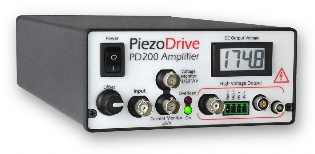
Figure 1: Picture of the PD200 Voltage Amplifier
The specifications as well as the amplifier characteristics as shown in the datasheet are summarized in Table 1.
| Characteristics | Manual | Specification |
|---|---|---|
| Input Voltage Range | +/- 10 [V] | +/- 10 [V] |
| Output Voltage Range | -50/150 [V] | -20/150 [V] |
| Gain | 20 [V/V] | |
| Maximum RMS current | 0.9 [A] | > 50 [mA] |
| Maximum Pulse current | 10 [A] | |
| Slew Rate | 150 [V/us] | |
| Noise (10uF load) | 0.7 [mV RMS] | < 2 [mV rms] |
| Small Signal Bandwidth (10uF load) | 7.4 [kHz] | > 5 [kHz] |
| Large Signal Bandwidth (150V, 10uF) | 300 [Hz] | > 1 [Hz] |
The most important characteristics are the large (small signal) bandwidth > 5 [kHz] and the small noise (< 2 [mV RMS]).
For a load capacitance of \(10\,\mu F\), the expected \(-3\,dB\) bandwidth is \(6.4\,kHz\) (Figure 2) and the low frequency noise is \(650\,\mu V\,\text{rms}\) (Figure 3).
These two characteristics are respectively measured in Section 3 and Section 4.
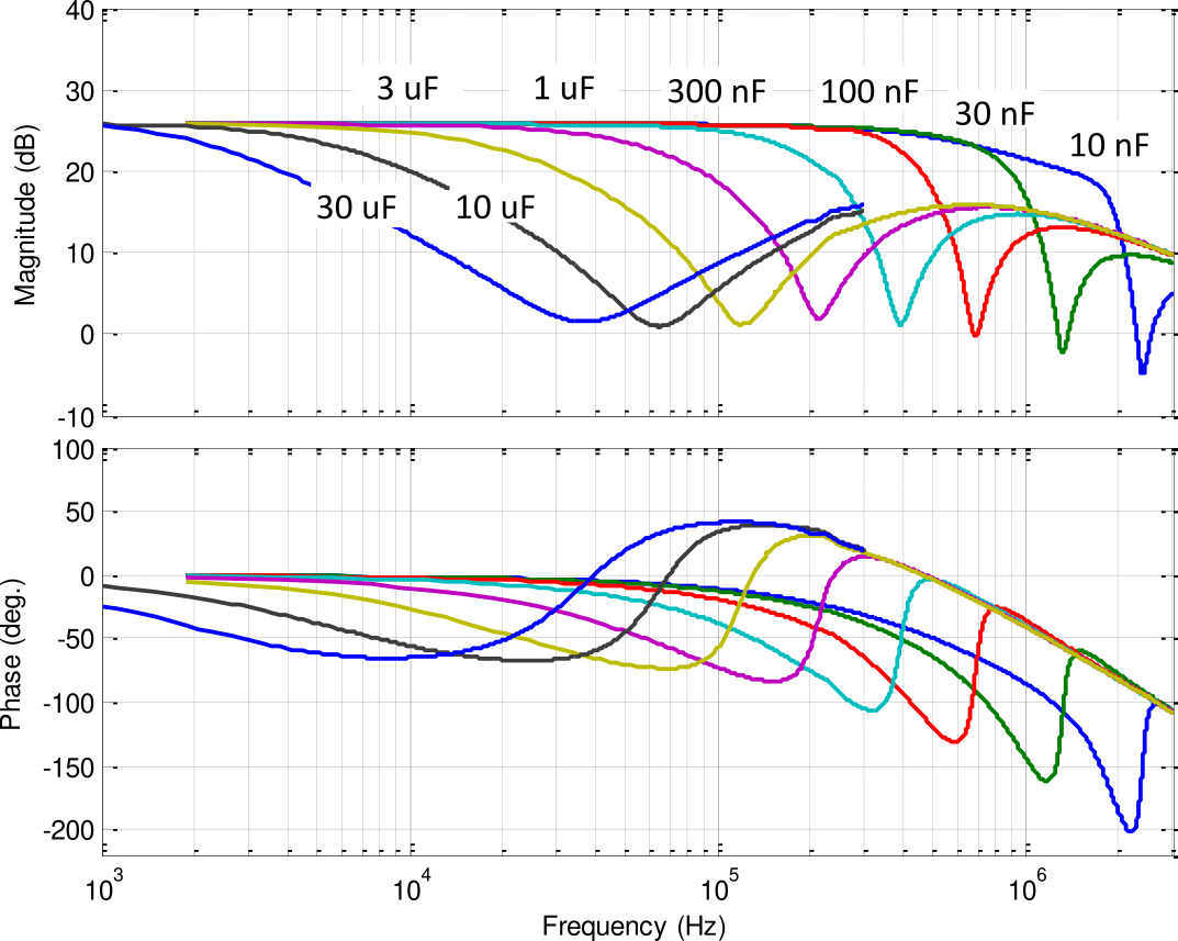
Figure 2: Expected small signal bandwidth
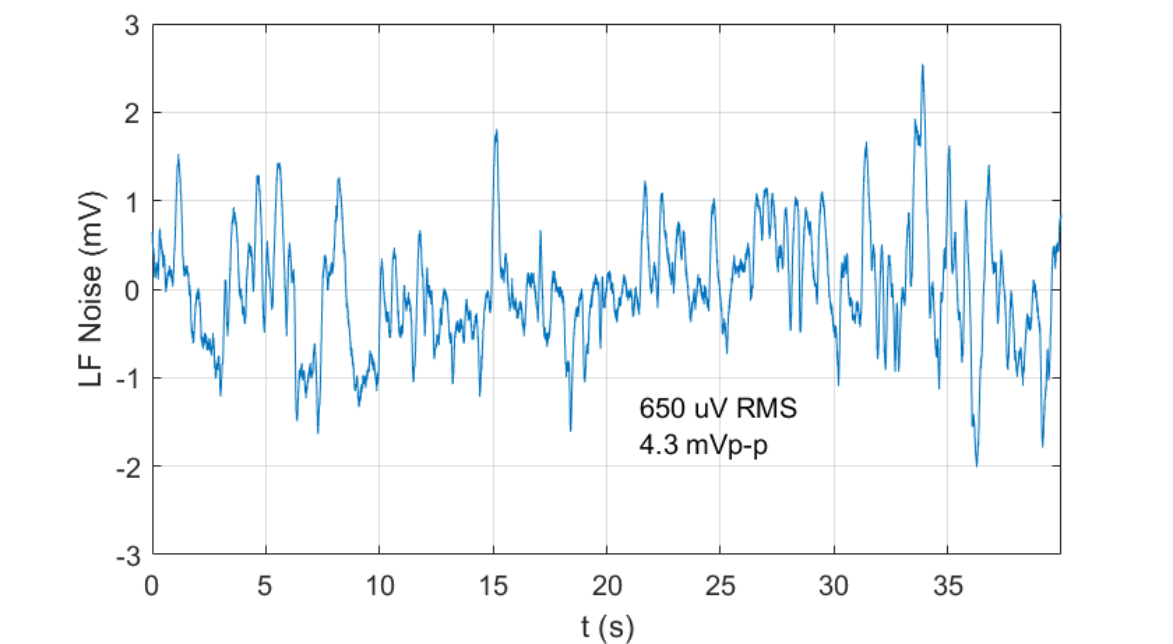
Figure 3: Expected Low frequency noise from 0.03Hz to 20Hz
2 Voltage Amplifier Model
The Amplifier is characterized by its dynamics \(G_p(s)\) from voltage inputs \(V_{in}\) to voltage output \(V_{out}\). Ideally, the gain from \(V_{in}\) to \(V_{out}\) is constant over a wide frequency band with very small phase drop.
It is also characterized by its input noise \(n\).
The objective is therefore to determine the transfer function \(G_p(s)\) from the input voltage to the output voltage as well as the Power Spectral Density \(S_n(\omega)\) of the amplifier input noise.
As \(G_p\) depends on the load capacitance, it should be measured when loading the amplifier with a \(10\,\mu F\) capacitor.
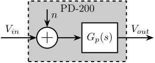
Figure 4: Model of the voltage amplifier
The input noise of the amplifier \(n\) can be further modeled by shaping a white noise with unitary PSD \(\tilde{n}\) with a transfer function \(G_n(s)\) as shown in Figure 6.
The Amplitude Spectral Density \(\Gamma_n\) is then:
\begin{equation} \Gamma_n(\omega) = |G_n(j\omega)| \Gamma_{\tilde{n}}(\omega) \end{equation}with \(\Gamma_{\tilde{n}}(\omega) = 1\).
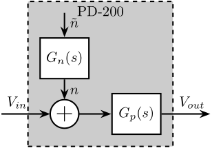
Figure 5: Model of the voltage amplifier with normalized noise input
3 Transfer Function measurement
In this section, the transfer function of the PD200 amplifier is measured:
- Section 3.1: the measurement setup is described
- Section 3.2: the maximum sinusoidal excitation frequency is estimated in order to not overload the amplifier
- Section 3.3: the small signal bandwidth measurement results are shown
- Section 3.4: a model of the small signal dynamics of the amplifier is obtained
- Section 3.5: the amplifier’s transfer function is estimated for several input amplitudes
3.1 Setup
In order to measure the transfer function from the input voltage \(V_{in}\) to the output voltage \(V_{out}\), the test bench shown in Figure 6 is used.
Here are the documentation of the equipment used for this test bench:
- Voltage Amplifier: PD200
- Load Capacitor: Film Capacitors 600V 10uF 5%
- DAC/ADC: IO313 Speedgoat Interface
For this measurement, the sampling frequency of the Speedgoat ADC should be as high as possible.
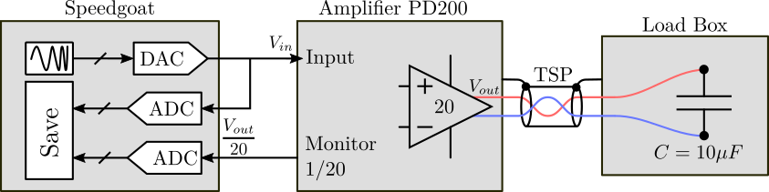
Figure 6: Schematic of the test bench to estimate the dynamics from voltage input \(V_{in}\) to voltage output \(V_{out}\)
3.2 Maximum Frequency/Voltage to not overload the amplifier
Then the maximum output current of the amplifier is reached, the amplifier automatically shuts down itself. We should then make sure that the output current does not reach this maximum specified current.
The maximum current is 1A [rms] which corresponds to 0.7A in amplitude of the sin wave.
The impedance of the capacitance is: \[ Z_C(\omega) = \frac{1}{jC\omega} \]
Therefore the relation between the output current amplitude and the output voltage amplitude for sinusoidal waves of frequency \(\omega\): \[ V_{out} = \frac{1}{C\omega} I_{out} \]
Moreover, there is a gain of 20 between the input voltage and the output voltage: \[ 20 V_{in} = \frac{1}{C\omega} I_{out} \]
For a specified voltage input amplitude \(V_{in}\), the maximum frequency at which the output current reaches its maximum value is:
\begin{equation} \boxed{\omega_{\text{max}} = \frac{1}{20 C V_{in}} I_{out,\text{max}}} \end{equation}with:
- \(\omega_{\text{max}}\) the maximum input sinusoidal frequency in Radians per seconds
- \(C\) the load capacitance in Farads
- \(V_{in}\) the input voltage sinusoidal amplitude in Volts
- \(I_{out,\text{max}}\) the specified maximum output current in Amperes
\(\omega_{\text{max}}/2\pi\) as a function of \(V_{in}\) is shown in Figure 7.
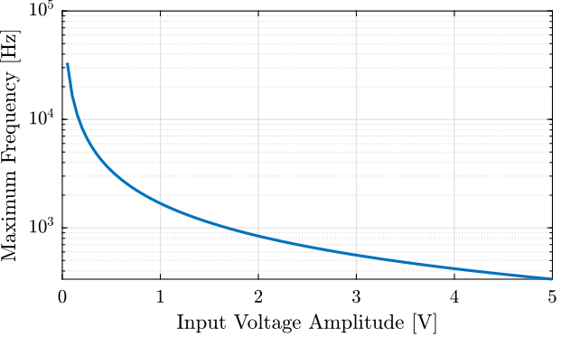
Figure 7: Maximum frequency as a function of the excitation voltage amplitude
When doing sweep sine excitation, we make sure not to reach this maximum excitation frequency.
3.3 Small Signal Bandwidth
Here the small signal dynamics of all the 7 PD200 amplifiers are identified.
A (logarithmic) sweep sine excitation voltage is generated by the Speedgoat DAC with an amplitude of 0.1V and a frequency going from 1Hz up to 5kHz.
The output voltage of the PD200 amplifier is measured thanks to the monitor voltage of the PD200 amplifier. The input voltage of the PD200 amplifier (the generated voltage by the DAC) is measured with another ADC of the Speedgoat. This way, the time delay related to the ADC will not be apparent in the results.
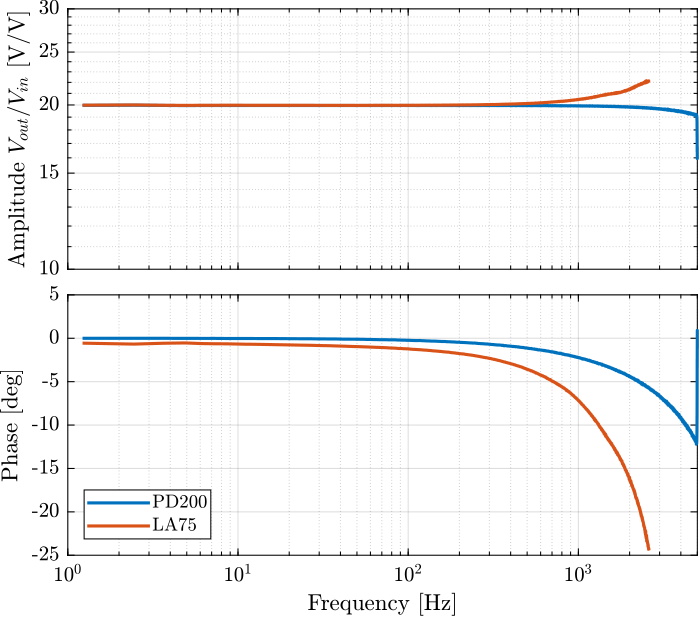
The obtained transfer functions from \(V_{in}\) to \(V_{out}\) are shown in Figure 8.
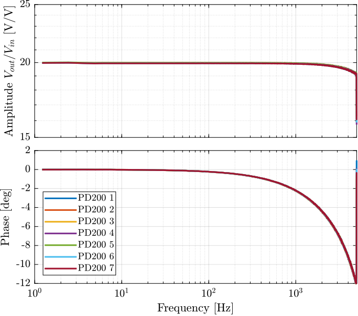
Figure 8: Identified dynamics from input voltage to output voltage
We can see the very well matching between all the 7 amplifiers. The amplitude is constant over a wide frequency band and the phase drop is limited to less than 1 degree up to 500Hz.
3.4 Model of the amplifier small signal dynamics
The identified dynamics in Figure 8 can very well be modeled this dynamics with a first order low pass filter (even a constant could work fine).
Below is the defined transfer function \(G_p(s)\).
Gp = 20/(1 + s/2/pi/25e3);
Comparison of the model with the identified dynamics is shown in Figure 9.
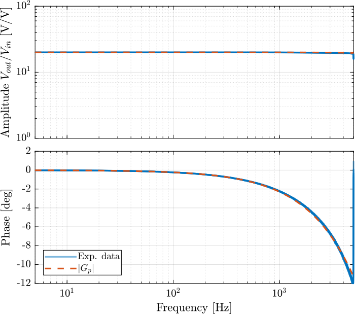
Figure 9: Bode plot of \(G_d(s)\) as well as the identified transfer functions of all 7 amplifiers
And finally this model is saved.
save('mat/pd200_model.mat', 'Gp');
3.5 Large Signal Bandwidth
The PD200 amplifiers will most likely not be used for large signals, but it is still nice to see how the amplifier dynamics is changing with the input voltage amplitude.
Several identifications using sweep sin were performed with input voltage amplitude ranging from 0.1V to 4V. The maximum excitation frequency for each amplitude was limited from the estimation in Section 3.2.
The obtained transfer functions for the different excitation amplitudes are shown in Figure 10. It is shown that the input voltage amplitude does not affect that much the amplifier dynamics.
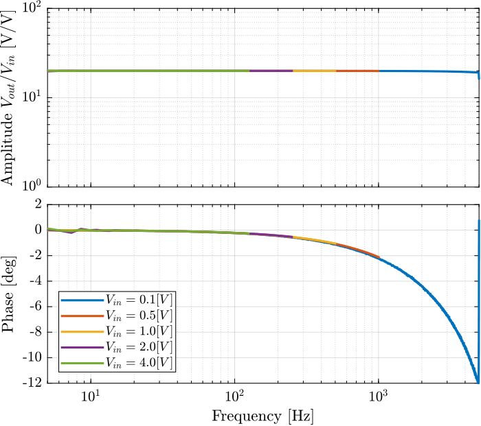
Figure 10: Amplifier dynamics for several input voltage amplitudes
4 Noise measurement
In this part, the goal is to measure the noise of the PD200 voltage amplifier. This noise can be separated into an input voltage noise and an input current noise. However, the input voltage noise has much larger effects than the input current noise and we will only try to measure the input voltage noise.
In section 4.1, the measurement setup is described and a model (block diagram) of the setup is given in section 4.2.
Then, the noise contribution of each element is measured:
- Section 4.3: the quantization noise of the ADC is estimated
- Sections 4.4 and 4.5: the noise of the low-noise amplifiers are estimated
- Sections 4.6 and 4.7:: the input voltage noise of the PD200 amplifier is estimated
- Section 4.8: the output noise of the DAC is measured
- Section 4.9: the noise of the full measurement chain (DAC to PD200 to pre-amplifier to ADC) is measured and it is found that the DAC is the main source of noise
- Section 4.10: the noise of an 20bits DAC is measured
- Section 4.11: it is shown if using the 20bits DAC could lower the overall noise of the setup
Finally in section 4.12, a model of the PD200 amplifier’s noise is developed.
Here are the documentation of the equipment used for this test bench:
- Voltage Amplifier PD200
- Load Capacitor: Film Capacitors 600V 10uF 5%
- Low Noise Voltage Amplifiers EG&G 5113 and Femto DLPVA
- ADC: IO313 Speedgoat card
- 16bits DAC: IO313 Speedgoat card
- 20bits DAC: SSI2V
4.1 Measurement Setup
As the output noise of the PD200 voltage amplifier is foreseen to be around 1mV rms in a bandwidth from DC to 1MHz, it is not possible to directly measure it with an ADC. We need to amplify the noise before digitizing the signal. To do so, we need to use a low noise voltage amplifier with a noise density much smaller than the measured noise of the PD200 amplifier.
Let’s first estimate the noise density of the PD200 amplifier. If we suppose a white noise, this correspond to an amplitude spectral density:
\begin{equation} \Gamma_{n}(\omega) \approx \frac{1\,mV}{\sqrt{1\,MHz}} = 1 \frac{\mu V}{\sqrt{Hz}} \end{equation}The input noise of the instrumentation amplifier should be then much smaller than the output noise of the PD200. We will use either the amplifier EG&G 5113 that has a noise of \(\approx 4 nV/\sqrt{Hz}\) referred to its input or the Femto DLPVA amplifier with an input noise of \(\approx 3nV/\sqrt{Hz}\).
The gain of the low-noise amplifier is then increased until the full range of the ADC is used. This gain should be around 1000 (60dB).
A representation of the measurement bench is shown in Figure 11.
Note that it is quite important to load the amplifier with the “Load Box” including a \(10\,\mu F\) capacitor as the (high frequency) noise of the amplifier depends on the actual load being used.
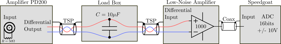
Figure 11: Schematic of the test bench to measure the Power Spectral Density of the Voltage amplifier noise \(n\)
4.2 Model of the setup
As shown in Figure 12, there are 4 elements involved in the measurement:
- a Digital to Analog Convert (DAC)
- the Voltage amplifier to be measured with a gain of 20 (PD200)
- a low noise voltage amplifier with a variable gain and integrated low pass filters and high pass filters
- an Analog to Digital Converter (ADC)
Each of these equipment has some noise:
- \(q_{da}\): quantization noise of the DAC
- \(n_{da}\): output noise of the DAC
- \(n_p\): input noise of the PD200 (what we wish to characterize)
- \(n_a\): input noise of the pre-amplifier
- \(q_{ad}\): quantization noise of the ADC

Figure 12: Sources of noise in the experimental setup
In the next sections, we wish to measure all these sources of noise and make sure that we can effectively characterize the noise \(n_p\) of the PD200 amplifier.
4.3 Quantization Noise of the ADC
The quantization noise is something that can be predicted from the sampling frequency and the quantization of the ADC. Indeed, the Amplitude Spectral Density of the quantization noise of an ADC/DAC is equal to:
\begin{equation} \Gamma_q(\omega) = \frac{q}{\sqrt{12 f_s}} \end{equation}with:
- \(q = \frac{\Delta V}{2^n}\) the quantization in [V], which is the corresponding value in [V] of the least significant bit
- \(\Delta V\) is the full range of the ADC in [V]
- \(n\) is the number of bits
- \(f_s\) is the sample frequency in [Hz]
Let’s estimate that with the ADC used for the measurements:
%% ADC Quantization noise
adc = struct();
adc.Delta_V = 20; % [V]
adc.n = 16; % number of bits
adc.Fs = 20e3; % [Hz]
adc.Gamma_q = adc.Delta_V/2^adc.n/sqrt(12*adc.Fs); % [V/sqrt(Hz)]
The obtained Amplitude Spectral Density is 6.2294e-07 \(V/\sqrt{Hz}\).
4.4 EG&G - Amplifier noise measurement
We now wish to measure the noise of the pre-amplifier. To do so, the input of the pre-amplifier is shunted with a 50Ohms resistor such that the pre-amplifier input voltage is just its input noise. Then, the gain of the amplifier is increased until the measured signal on the ADC is much larger than the quantization noise.
The Amplitude Spectral Density \(\Gamma_n(\omega)\) of the measured signal \(n\) is computed. Finally, the Amplitude Spectral Density of \(n_a\) can be computed taking into account the gain of the pre-amplifier:
\begin{equation} \Gamma_{n_a}(\omega) \approx \frac{\Gamma_n(\omega)}{|G_a(\omega)|} \end{equation}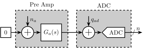
Figure 13: Sources of noise in the experimental setup
The gain of the low noise amplifier is set to 50000 for the measurement.
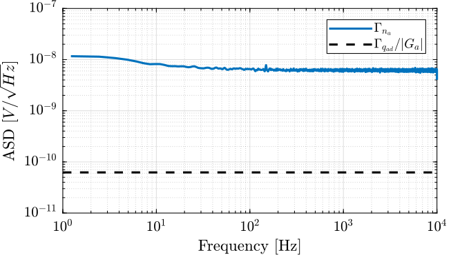
The obtained Amplitude Spectral Density of the Low Noise Voltage Amplifier is shown in Figure 14. The obtained noise amplitude is very closed to the one specified in the documentation of \(4nV/\sqrt{Hz}\) at 1kHZ.
It is also verified that the quantization noise of the ADC is much smaller and what we are measuring is indeed the noise of the pre-amplifier.

Figure 14: Obtained Amplitude Spectral Density of the EG&G Low Noise Voltage Amplifier
4.5 Femto - Amplifier noise measurement
4.6 PD200 - Low frequency noise measurement
The measurement setup is shown in Figure 16. The input of the PD200 amplifier is shunted with a 50 Ohm resistor such that there in no voltage input expected the PD200 input voltage noise. The gain of the pre-amplifier is increased in order to measure a signal much larger than the quantization noise of the ADC.

Figure 16: Sources of noise in the experimental setup
The measured low frequency (<20Hz) output noise of one of the PD200 amplifiers is shown in Figure 17. It is very similar to the one specified in the datasheet in Figure 3.
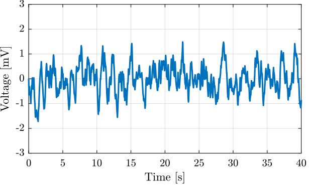
Figure 17: Measured low frequency noise of the PD200 from 0.01Hz to 20Hz
The obtained RMS and peak to peak values of the measured output noise are shown in Table 2 and found to be very similar to the specified ones.
| RMS [\(\mu V\)] | Peak to Peak [\(mV\)] | |
|---|---|---|
| Specification [\(10\,\mu F\)] | 714.0 | 4.3 |
| PD200 1 | 565.1 | 3.7 |
| PD200 2 | 767.6 | 3.5 |
| PD200 3 | 479.9 | 3.0 |
| PD200 4 | 615.7 | 3.5 |
| PD200 5 | 651.0 | 2.4 |
| PD200 6 | 473.2 | 2.7 |
| PD200 7 | 423.1 | 2.3 |
4.7 PD200 - High frequency noise measurement
The measurement setup is the same as in Figure 16.
The Amplitude Spectral Density \(\Gamma_n(\omega)\) of the measured signal by the ADC is computed. The Amplitude Spectral Density of the input voltage noise of the PD200 amplifier \(n_p\) is then computed taking into account the gain of the pre-amplifier and the gain of the PD200 amplifier:
\begin{equation} \Gamma_{n_p}(\omega) = \frac{\Gamma_n(\omega)}{|G_p(j\omega) G_a(j\omega)|} \end{equation}And we verify that we are indeed measuring the noise of the PD200 and not the noise of the pre-amplifier by checking that:
\begin{equation} \Gamma_{n_p}(\omega) |G_p(j\omega)| \ll \Gamma_{n_a} \end{equation}The Amplitude Spectral Density of the measured input noise is computed and shown in Figure 18.
It is verified that the contribution of the PD200 noise is much larger than the contribution of the pre-amplifier noise of the quantization noise.
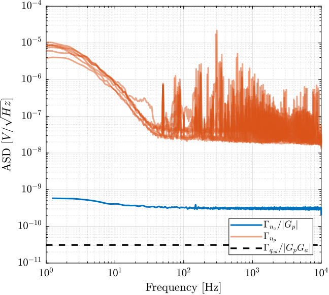
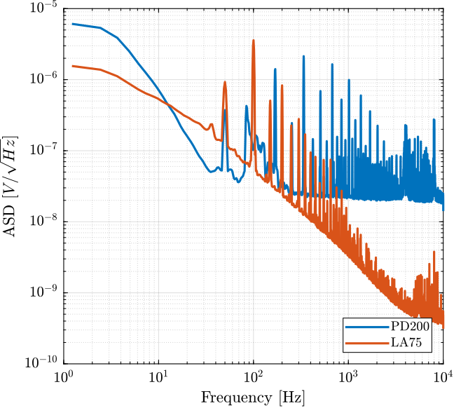
Figure 18: Amplitude Spectral Density of the measured input voltage noise of the PD200 amplifiers
The Amplitude Spectral Density of the input noise of the PD200 amplifiers present sharp peaks. It is not clear yet what causes such peaks and if these peaks have high influence on the total RMS noise of the amplifiers.
4.8 16bits DAC noise measurement
In order not to have any quantization noise and only measure the output voltage noise of the DAC, we “ask” the DAC to output a zero voltage.
The measurement setup is schematically represented in Figure 19. The gain of the pre-amplifier is adjusted such that the measured amplified noise is much larger than the quantization noise of the ADC.
The Amplitude Spectral Density \(\Gamma_n(\omega)\) of the measured signal is computed. The Amplitude Spectral Density of the DAC output voltage noise \(n_{da}\) can be computed taking into account the gain of the pre-amplifier:
\begin{equation} \Gamma_{n_{da}}(\omega) = \frac{\Gamma_m(\omega)}{|G_a(\omega)|} \end{equation}And it is verified that the Amplitude Spectral Density of \(n_{da}\) is much larger than the one of \(n_a\):
\begin{equation} \Gamma_{n_{da}} \gg \Gamma_{n_a} \end{equation}
Figure 19: Sources of noise in the experimental setup
The obtained Amplitude Spectral Density of the DAC’s output voltage is shown in Figure 20.
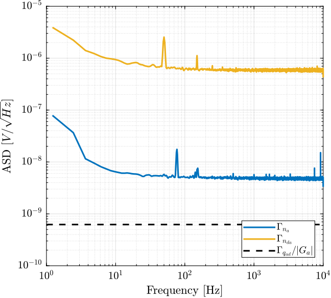
Figure 20: Amplitude Spectral Density of the measured output voltage noise of the 16bits DAC
4.9 Noise of the full setup with 16bits DAC
Let’s now measure the noise of the full setup in Figure 21 and analyze the results.
Figure 21: Sources of noise in the experimental setup
The Amplitude Spectral Density of the measured noise is computed and the shown in Figure 22.
We can very well see that to total measured noise is the sum of the DAC noise and the PD200 noise.
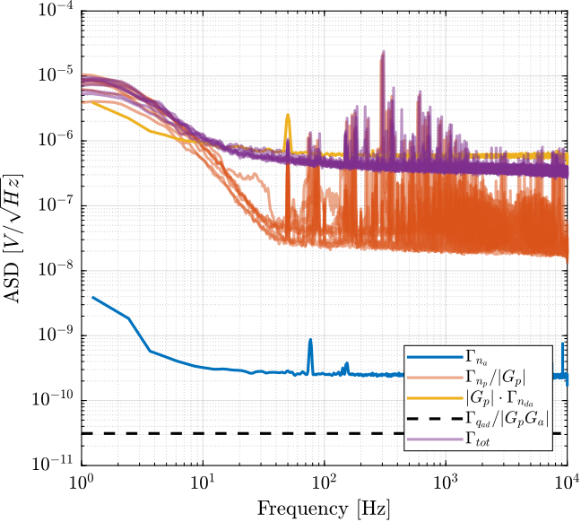
Figure 22: Amplitude Spectral Density of the measured noise and of the individual sources of noise
The input noise of the PD200 amplifier is limited by the output voltage noise of the DAC. Having a DAC with lower output voltage noise could lower the overall noise of the setup. SSI2V 20bits DACs are used in the next section to verify that.
4.10 20bits DAC noise measurement
Let’s now measure the output voltage noise of another DAC called the “SSI2V” (doc). It is a 20bits DAC with an output voltage range of +/-10.48 V and a very low output voltage noise.
The measurement setup is the same as the one in Figure 19.
The obtained Amplitude Spectral Density of the output voltage noise of the SSI2V DAC is shown in Figure 23 and compared with the output voltage noise of the 16bits DAC. It is shown to be much smaller (~1 order of magnitude).
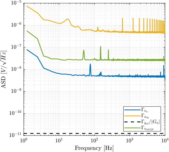
Figure 23: Amplitude Spectral Density of the SSI2V DAC’s noise
Using the SSI2V as the DAC with the PD200 should give much better noise output than using the 16bits DAC. The limiting factor should then be the noise of the PD200 itself.
4.12 PD200 Amplifier noise model
Let’s design a transfer function \(G_n(s)\) whose norm represent the Amplitude Spectral Density of the input voltage noise of the PD200 amplifier as shown in Figure 24.
Figure 24: Model of the voltage amplifier with normalized noise input
A simple transfer function that allows to obtain a good fit is defined below.
%% Model of the PD200 Input Voltage Noise
Gn = 1e-5 * ((1 + s/2/pi/20)/(1 + s/2/pi/2))^2 /(1 + s/2/pi/5e3);
The comparison between the measured ASD of the modeled ASD is done in Figure 25.
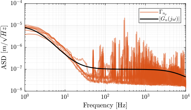
Figure 25: ASD of the measured input voltage noise and modeled noise using \(G_n(s)\)
Let’s now compute the Cumulative Amplitude Spectrum corresponding to the measurement and the model and compare them.
The integration from low to high frequency and from high to low frequency are both shown in Figure 26.
The fit between the model and the measurements is rather good considering the complex shape of the measured ASD and the simple model used.
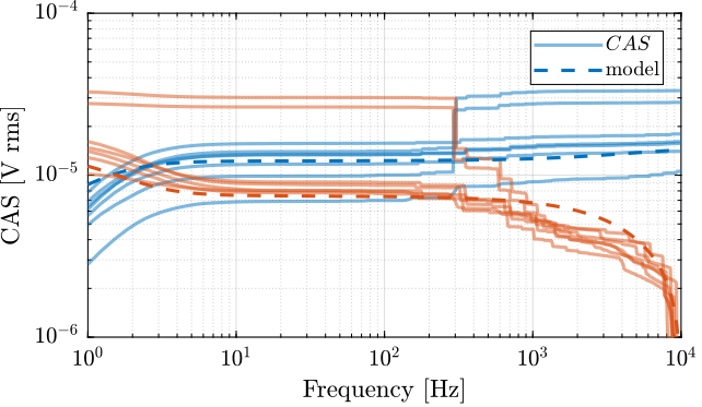
Figure 26: Cumulative Amplitude Spectrum of the measured input voltage noise and modeled noise using \(G_n(s)\)
The obtained RMS noise of the model is 286.74 uV RMS which is not that far from the specifications.
Finally the model of the amplifier noise is saved.
save('mat/pd200_model.mat', 'Gn', '-append');
5 Output Impedance
The goal of this experimental setup is to estimate the output impedance \(R_\text{out}\) of the PD200 voltage amplifiers. A DAC with a constant output voltage (here 0.1V) is connected to the input of the PD200 amplifier.
Then, the output voltage of the PD200 amplifier is measured in two conditions:
- \(V\) when the output is not connected to any load
- \(V_p\) when a load \(R = 10\,\Omega\) is connected at the output of the amplifier
The load and the output impedance form a voltage divider, and thus: \[ V^\prime = \frac{R}{R + R_\text{out}} V \]
From the two values of voltage, the output impedance of the amplifier can be estimated: \[ R_\text{out} = R \frac{V - V^\prime}{V^\prime} \]
A schematic of the setup is shown in Figure 27.
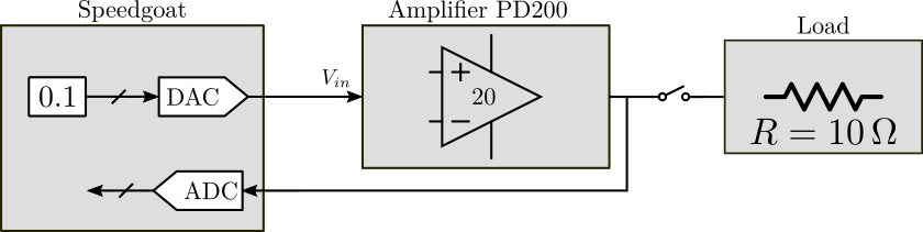
Figure 27: Schematic of the setup use to estimate the output impedance of the PD200 amplifier
Below are defined the measured output voltages with and without the 10Ohm load:
R = 10; % Load [Ohm]

%       V      Vp
meas = [1.988, 1.794; % PD200 - 1
        1.990, 1.789; % PD200 - 2
        1.982, 1.795; % PD200 - 3
        1.984, 1.789; % PD200 - 4
        1.998, 1.810; % PD200 - 5
        1.984, 1.799; % PD200 - 6
        2.004, 1.812] % PD200 - 7
The output impedance of the amplifier can then be estimated using:
\begin{equation} R_{\text{out}} = R_{\text{load}} \frac{V - V_p}{V} \end{equation}meas(:, 3) = R * (meas(:,1) - meas(:,2))./meas(:,2)
The obtained output impedances are shown in Table 3.
| PD200 | \(V\ [V]\) | \(V_p\ [V]\) | \(R_\text{out}\ [\Omega]\) |
|---|---|---|---|
| 1 | 1.988 | 1.794 | 1.081 |
| 2 | 1.99 | 1.789 | 1.124 |
| 3 | 1.982 | 1.795 | 1.042 |
| 4 | 1.984 | 1.789 | 1.09 |
| 5 | 1.998 | 1.81 | 1.039 |
| 6 | 1.984 | 1.799 | 1.028 |
| 7 | 2.004 | 1.812 | 1.06 |
The output impedance of the PD200 Amplifier is estimated to be \(\approx 1\,\Omega\).
6 Comparison to other commercial amplifiers
6.1 Introduction
In this section, three similar voltage amplifiers are compared:
These are compared in term of dynamic from input voltage to output voltage for a load of \(10\,\mu F\) in Section 6.2 and then in term of input voltage noise in Section 6.3.
The characteristics that I could find for the three amplifiers are summarized in Table 4.
| Characteristics | PD200 | LA75B | E-505 |
|---|---|---|---|
| Gain | 20 [V/V] | 20 [V/V] | 10 [V/V] |
| Maximum RMS current | 0.9 [A] | 0.4 [A] | |
| Maximum Pulse current | 10 [A] | 1 [A] | 2 [A] |
| Slew Rate | 150 [V/us] | ||
| Noise (10uF load) | 0.7 [mV RMS] | 3.4 [mV RMS] | 0.6 [mV RMS] |
| Small Signal Bandwidth | 7.4 [kHz] (10uF) | 30 [kHz] (unloaded) |
6.2 Transfer functions
7 Conclusion
| Characteristics | Measurement | Manual | Specification |
|---|---|---|---|
| Input Voltage Range | - | +/- 10 [V] | +/- 10 [V] |
| Output Voltage Range | - | -50/150 [V] | -20/150 [V] |
| Gain | 20 [V/V] | - | |
| Maximum RMS current | 0.9 [A] | > 50 [mA] | |
| Maximum Pulse current | 10 [A] | - | |
| Slew Rate | 150 [V/us] | - | |
| Noise (10uF load) | 0.7 [mV RMS] | < 2 [mV rms] | |
| Small Signal Bandwidth (10uF load) | 7.4 [kHz] | > 5 [kHz] | |
| Large Signal Bandwidth (150V, 10uF) | 300 [Hz] | - |